



UNPARALLELED, a professional supplier of ultra‑precision structural components, delivers high‑stability granite platforms tailored for wafer inspection systems, helping semiconductor customers obtain repeatable and trustworthy defect‑testing results in clean‑room environments.
Wafer inspection puts forward harsh requirements for base stability. Even faint vibration and subtle temperature shift may interfere with optical imaging, causing misjudgment of tiny chip defects. Serving as the foundational substrate of inspection machines, granite platforms support the installation of optical assemblies, sensing units and auxiliary metrology accessories.
Premium black granite raw material is adopted for these platforms. With natural low thermal‑expansion property and superior vibration absorption performance, the material goes through sufficient natural aging to remove internal stress. Fine manual lapping secures superior flatness and geometric consistency for long‑term continuous operation. Pre‑formed mounting holes, positioning grooves and T‑slots allow direct assembly with precision adjustment brackets and metrology gauges including V‑blocks, avoiding extra rework at customer sites. 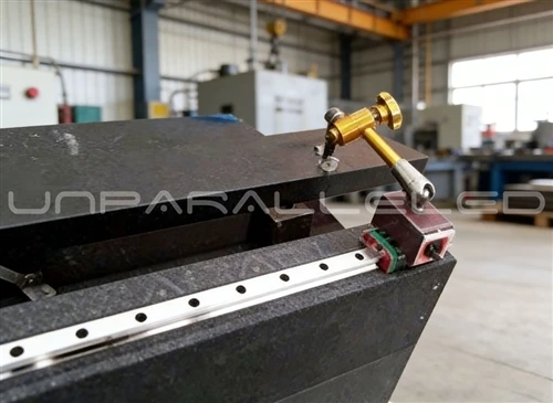
Every granite platform is manufactured under ISO and CE quality management frameworks. Finished goods are fully examined with metrology tools traceable to CNAS standards, and official inspection certificates can be provided upon request. The platforms maintain steady performance under round‑the‑clock operation and effectively suppress positioning drift during wafer scanning processes.
Drawing on abundant project experience with world‑famous enterprises and research institutes, UNPARALLELED offers full‑set services covering technical evaluation, material selection, precision finishing, performance verification and safe shipment. Custom dimensions and structural layouts are available to fit different wafer‑inspection equipment layouts.
For semiconductor clean‑room working conditions, low‑deformation granite platforms minimize outside disturbances. They act as dependable foundational structures for high‑accuracy wafer defect detection tasks.