



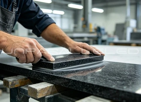
Not every piece of semiconductor process equipment has the same structural needs, and this article is deliberately narrow in scope: it covers structural granite bases and precision mounting interfaces inside semiconductor equipment - the platform on which stages, rails, sensors and process modules are mounted. Metrology frames, motion platforms and inspection devices each raise their own questions, and lumping all "semiconductor equipment" together hides the decisions that actually matter.
A design review is where those decisions surface. Before we machine a single slab for a granite base for semiconductor equipment, our engineering team works through the questions below with the customer. Use them as a checklist for your own design review.
1. Which surfaces are assembly or measuring datums?
A granite base usually has one primary top surface plus several secondary interfaces. The review question is which surfaces the customer will actually measure and assemble against - and in what order. Datum hierarchy drives machining sequence, so we confirm it on the drawing before quoting, not after machining.
2. Overall flatness, or flatness in defined zones?
Customers often ask for "0.005 mm flatness" without specifying whether it applies to the entire surface or only to the areas under the stage and rails. In many designs, full-surface tolerance can be relaxed while critical zones are tightened, which shortens lapping time and lowers cost. Our review always pins this down: which zones, what tolerance, measured over what area.
3. How is the base supported and loaded?
Three-point support is kinematically clean; multi-point or full-face support can better distribute heavy stage loads but requires flatness at the support locations. Stage weight, moving-axis reactions and point loads from process modules all affect the choice. We also confirm whether the base sits on isolation mounts, air bearings or a steel frame, because the interface design follows from it.
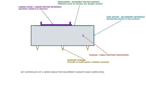
The simplified diagram above shows the interfaces our review covers: the measuring and assembly datum surface, the linear guide and linear motor interfaces, the secondary side datum, the support scheme and provisions for sensors and cable routing.
4. How are rails, linear motors and sensors mounted?
Guide rails and linear motors need position accuracy relative to the datums, threaded inserts in defined materials, and sometimes intermediate steel plates for thermal or wear reasons. Sensors and cable chains need pockets, channels and clean routing that does not interfere with the moving stage. Each of these is checked for manufacturability in granite - insert depth, edge distances and minimum wall thickness included.
5. What are the cleanliness, handling and assembly requirements?
Semiconductor assembly environments impose real constraints: no dust-generating defects, defined cleaning before shipment, lifting points that do not damage lapped surfaces, and packaging that survives export transport without contaminating the part. We confirm these with the customer together with the delivery schedule, because they change the process plan.
6. What are the acceptance conditions and methods?
Instead of promising that "all semiconductor bases reach the same precision", we agree in advance on what will be measured, with which instrument, and what the report will show: flatness maps per zone, parallelism of side datums, insert torque tests if required, and a final inspection report shipped with the base. The acceptance sheet is part of the design review output, not an afterthought.
A project fragment: from question to verified delivery
In a recent project for an inspection equipment integrator, the customer's drawing called for "flatness 0.005 mm" across a 1,900 x 1,400 mm top surface, and the quotation they received from several suppliers assumed full-surface lapping. During our design review we asked which regions actually carried the stage and rails. The customer confirmed that only two rail zones and the stage mounting area were functional measuring references. We proposed zoned tolerances, the customer's engineering team verified the load mapping, and the agreed drawing revision reflected it.
Machining followed the revised plan: rough milling, stress relaxation, then precision lapping concentrated on the critical zones. Before shipment, the customer received the flatness measurement report for each defined zone, taken on our inspection equipment at 20 C, together with photographs of the packed base. The part passed the customer's incoming inspection without a single deviation report - and the review process, not the promise, is what made that possible.
Similar interface thinking applies across our semiconductor granite components and measuring machine platforms, whether the base is a single slab or a multi-piece granite assembly.
If you are designing or integrating semiconductor equipment, send us your application description, installation interfaces and drawings. Our engineering team will review them with you, raise the questions above before they become costly changes, and propose a manufacturing and inspection plan for the project.